Perhimpunan PCB
Pengalaman pembuatan elektronik hampir 15 tahun
SATECH menyediakan perkhidmatan pemasangan PCB sehenti untuk pembuatan elektronik, daripada sumber komponen, Pengeluaran PCB, SMT, DIP, Pemasangan PCB kepada pemasangan produk siap. Dengan keunggulan pembelian secara besar-besaran (daripada IC, rintangan, kemuatan, kearuhan, diod dan audion,dan lain-lain.) dan kualiti-rasa pertama, kami membuat kontrak dengan pengeluar komponen yang sangat baik dari rumah dan di atas kapal untuk membina perkongsian jangka panjang, ini memastikan kualiti asli dan bekalan yang stabil, bertujuan untuk menyampaikan manfaat kepada pelanggan kami. Kami telah bekerja untuk pelanggan dari AS, Jerman, Rusia, Yaman, UAE, Jepun, Sepanyol, Perancis, Itali, Israel, Iran, India, Mexico, Argentina, Colombia, dan lain-lain.
Penyelesaian Perhimpunan Papan PCB Turnkey
- Pemulihan cepat
- Sokongan Prototaip/Pengeluaran
- Papan kosong »Komponen» Perhimpunan
- Petikan dalam talian yang cepat
Sejak bermula 2003, Satech telah muncul sebagai pengeluar kontrak elektronik yang boleh dipercayai (ECM) Untuk memenuhi permintaan penyelesaian pemasangan PCB yang cepat. Tidak kira sama ada ia adalah pesanan sampel atau pesanan pukal, Kami sentiasa berkesan untuk mengkaji dan menganalisis fail bom dan teknikal, dan komponen sumber cepat untuk petikan pesat. Untuk langkah pengeluaran dan QC, Beberapa peraturan dan peraturan yang ketat dan KPI disediakan untuk setiap pengurus dan pekerja kemudahan. Tiada kualiti untuk anda, tiada kehidupan untuk kita.
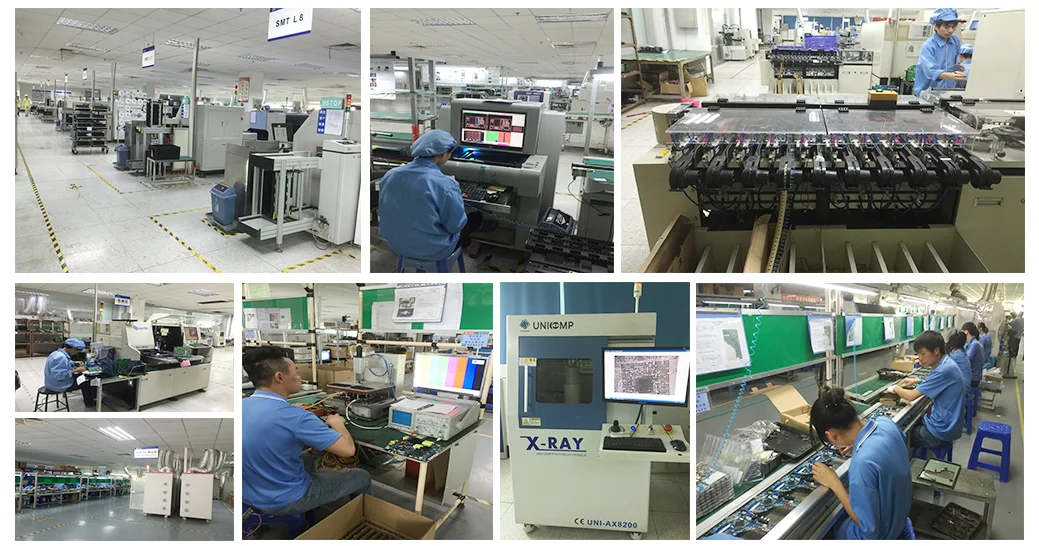
| Keupayaan pembuatan | Perkhidmatan pemasangan PCB | Senarai Kemudahan |
|---|---|---|
| 4 Garis pemprosesan SMT | Pengeluaran papan litar (sehingga 12 lapisan, impedans, HDI, dan lain-lain.) | Mesin Permukaan Surface-Mount Siri Fuji CP8 |
| 3 Garis pemprosesan | SMT/DIP | Pencetak solder-paste automatik |
| 0201 Komponen Assy | ICT (Ujian dalam litar) | 10-Pematerian aliran semula zon |
| 0.25mm bga | Fct (Ujian litar fungsional) | Pengesan AOI |
| Permukaan-permukaan 4 juta pin/hari | Bit (Ujian terbakar) | Gelombang-solder |
| DIP 1 juta pin/hari | Bangunan kotak | Platform kerja ICT |
Keupayaan pemasangan PCB yang disokong
- Thd (Peranti melalui lubang)
- SMT (Teknologi Surface-Mount)
- SMT & THD digabungkan
- 2-SMT dan pemasangan Thd
- 1 kepada 5,000 papan
- Bahagian pasif, saiz terkecil 0201
- Padang halus ke 8 Mil
- BGA, uBGA, Qfn, Cip pop dan sifar
- Penyambung dan terminal
- Gulungan
- Potong pita
- Tiub dan dulang
- Bahagian longgar dan pukal
- Pengukuran minimum: 0.2"X 0.2" (5mm x 5mm)
- Dimensi terbesar: 15"X 20" (381mm x 508mm)
- Bujur
- Bulat
- Slot dan potong
- Rumit dan tidak biasa
- Papan FR-4 tegar
- Papan tegar-flex
- Proses yang dipimpin
- Sifar-memimpin (ROHS)
- Gerber RS-274X, 274D, Eagle serta DXF AutoCAD, DWG
- Bom (Rang Undang -Undang Bahan) (.XLS, .CSV, . XLSX)
- Centroid (Fail pick-n-tempat atau xy)
- Pemeriksaan visual
- Pemeriksaan X-ray
- Aoi (Juga dikenali sebagai: Pemeriksaan optik automatik)
- ICT (Aka: Ujian dalam litar)
- Ujian fungsional
- 1 Ke 5 Hari untuk hanya papan litar bercetak Assy
- 10 Hingga16 hari untuk kad litar turnkey penuh Assy


")


