PCB Assembly
Nearly 15-year Experience of Electronics Manufacturing
SATECH provides one-stop PCB assembly services for electronics manufacturing, from components sourcing, PCB production, SMT, DIP, PCB assembly to finished-product assembly. With the superiority of large-scale purchasing (of IC, resistances, capacitance, inductance, diode and audion,etc.) and quality-first sense, we contract with the excellent component manufacturers from home and aboard to build long-term partnership, this makes sure of original quality and stable supply, aiming at transmitting the benefit to our clients. We have been working for the clients from US, Germany, Russia, Yemen, UAE, Japan, Spain, France, Italy, Israel, Iran, India, Mexico, Argentina, Colombia, etc.
Turnkey PCB Board Assembly Solutions
- Rapid Turnaround
- Prototype/Production Support
- Blank Boards » Components » Assembly
- Rapid On-line Quote
Since starting in 2003, SATECH has emerged as a trustworthy electronic contract manufacturer (ECM) to meet the demand of fast turnkey PCB assembly solutions. No matter whether it is a sample order or bulk order, we are always effective at reviewing and analyzing BOM and technical files, and quick to source components for rapid quotation. For the production and QC steps, some strict rules and regulations and KPI are available for every facility manager and worker. No quality for you, no life for us.
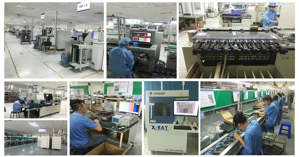
| Ability of manufacturing | PCB Assembly Service | Facility List |
|---|---|---|
| 4 SMT processing lines | Circuit board production (up to 12 layers, impedance, HDI, etc.) | Fuji CP8 Series Surface-mount Machine |
| 3 DIP processing lines | SMT/DIP | Automated solder-paste printer |
| 0201 components assy | ICT (In-Circuit Test) | 10-zone Re-flow Soldering |
| 0.25mm BGA | FCT (Functional Circuit Test) | AOI Detector |
| Surface-mount 4 million pins/day | BIT (Burn-in Test) | Wave-soldering |
| DIP 1 million pins/day | Box Building | ICT Working Platform |
Supported PCB Assembly Capabilities
- THD (Thru-Hole Device)
- SMT (Surface-Mount Technology)
- SMT & THD combined
- 2-sided SMT and THD assembly
- 1 to 5,000 boards
- Passives parts, smallest size 0201
- Fine pitch to 8 Mils
- BGA, uBGA, QFN, POP and Zero-Lead chips
- Connectors and terminals
- Reels
- Cut tape
- Tube and tray
- Loose parts and bulk
- Minimum measurement: 0.2″ x 0.2″ (5mm x 5mm)
- Largest dimension: 15″ x 20″ (381mm x 508mm)
- Oblong
- Round
- Slots and Cut outs
- Complicated and Uncommon
- Rigid FR-4 boards
- Rigid-Flex boards
- Leaded process
- Zero-Lead (RoHS)
- Gerber RS-274X, 274D, Eagle as well as AutoCAD’s DXF, DWG
- BOM (Bill of Materials) (.xls, .csv, . xlsx)
- Centroid (Pick-N-Place Or XY file)
- Visual Inspection
- X-ray Inspection
- AOI (Also known as: Automated Optical Inspection)
- ICT (AKA: In-Circuit Test)
- Functional testing
- 1 To 5 days for only printed circuit board assy
- 10 To16 days for full Turnkey Circuit Card Assy


")


